main page
download
FAQ
research notes
data sheets
schematics
hardware mods
mailing list
IRC
tools
photos
daily builds
CVS
sourceforge
linux driver
Jukebox notes
Exception vectors
The first 0x200 bytes of the image appears to be the exception vector table. The vectors are explained on pages 54 and 70-71 in the SH-1 Hardware Manual,
Here's the vector table for v5.03a:
| Vector | Address | Description/interrupt source |
|---|---|---|
| 0 | 09000200 | Power-on reset PC |
| 1 | 0903f2bc | Power-on reset SP |
| 2 | 09000200 | Manual reset PC |
| 3 | 0903f2bc | Manual reset SP |
| 11 | 09000cac | NMI |
| 64 | 0900c060 | IRQ0 |
| 70 | 09004934 | IRQ6 |
| 78 | 09004a38 | DMAC3 DEI3 |
| 80 | 0900dfd0 | ITU0 IMIA0 |
| 88 | 0900df60 | ITU2 IMIA2 |
| 90 | 0900df60 | ITU2 OVI2 |
| 104 | 09004918 | SCI1 ERI1 |
| 105 | 090049e0 | SCI1 Rxl1 |
| 109 | 09010270 | A/D ITI |
From the use of address 0x0903f2bc as stack pointer, we can deduce that the DRAM is located at address 0x09000000. This is backed by the HW manual p102, which says that DRAM can only be at put on CS1, which is either 0x01000000 (8-bit) or 0x09000000 (16-bit).
The vector table also corresponds with the fact that there is code at address 0x200 of the image file. 0x200 is thus the starting point for all code.
Port pins
|
Port A pin function configuration summary:
|
Port B pin function configuration summary:
|
Port C pin function configuration summary:
| Pin | Function | Input/output | Used for |
|---|---|---|---|
| PC0 | i/o | Input | Key: - / PREV |
| PC1 | i/o | Input | Key: MENU |
| PC2 | i/o | Input | Key: + / NEXT |
| PC3 | i/o | Input | Key: PLAY |
| PC4 | i/o | Input | |
| PC5 | i/o | Input | |
| PC6 | i/o | Input | |
| PC7 | i/o | Input |
Labels
Note: Everything is about v5.03a.
- 0x0200: Start point
- 0x383d: Text: "Archos Jukebox hard drive is not bootable! Please insert a bootable floppy and press any key to try again" :-)
- 0xc390: Address of "Update" string shown early on LCD.
- 0xc8c0: Start of setup code
- 0xc8c8: DRAM setup
- 0xc4a0: Serial port 1 setup
- 0xc40a: Port configuration setup
- 0xe3bc: Character set conversion table
- 0xfcd0: ITU setup
- 0xc52a: Memory area #6 setup
- 0x114b0: Start of menu strings
Setup
The startup code at 0x200 (0x09000200) naturally begins with setting up the system.
Vector Base Register
The first thing the code does is setting the VBR, Vector Base Register, and thus move the exception vector table from the internal ROM at address 0 to the DRAM at address 0x09000000:
0x00000200: mov.l  @(0x02C,pc),r1  ; 0x0000022C (0x09000000)
0x00000202: ldc	   r1,vbr
Stack
The next instruction loads r15 with the contents of 0x228, which is 0x0903f2bc. This is the stack pointer, which is used all over the code.
0x00000204: mov.l @(0x024,pc),r15 ; 0x00000228 (0x0903F2BC)
After that the code jumps to the hardware setup at 0xc8c0.
0x00000206: mov.l  @(0x01C,pc),r0   ; 0x00000220 (0x0900C8C0)
0x00000208: jsr    @r0
DRAM controller
First up is DRAM setup, at 0xc8c8. It sets the memory controller registers:
0x0000C8C8: mov.l  @(0x068,pc),r2  ; 0x0000C930 (0x05FFFFA8)
0x0000C8CA: mov.w  @(0x05A,pc),r1  ; 0x0000C924 (0x1E00)
0x0000C8CC: mov.l  @(0x068,pc),r7  ; 0x0000C934 (0x0F0001C0)
0x0000C8CE: mov.w  r1,@r2          ; 0x1e00 -> DCR
0x0000C8D0: mov.l  @(0x068,pc),r2  ; 0x0000C938 (0x05FFFFAC)
0x0000C8D2: mov.w  @(0x054,pc),r1  ; 0x0000C926 (0x5AB0)
0x0000C8D4: mov.w  r1,@r2          ; 0x5ab0 -> RCR
0x0000C8D6: mov.l  @(0x068,pc),r2  ; 0x0000C93C (0x05FFFFB2)
0x0000C8D8: mov.w  @(0x050,pc),r1  ; 0x0000C928 (0x9605)
0x0000C8DA: mov.w  r1,@r2          ; 0x9505 -> RTCOR
0x0000C8DC: mov.l  @(0x064,pc),r2  ; 0x0000C940 (0x05FFFFAE)
0x0000C8DE: mov.w  @(0x04C,pc),r1  ; 0x0000C92A (0xA518)
0x0000C8E0: mov.w  r1,@r2          ; 0xa518 -> RTCSR
Serial port 0
Code starting at 0x483c.
As C code:
void setup_sci0(void)
{
    /* set PB12 to output */
    PBIOR |= 0x1000;

    /* Disable serial port */
    SCR0 = 0x00;

    /* Syncronous, 8N1, no prescale */
    SMR0 = 0x80;

    /* Set baudrate 1Mbit/s */
    BRR0 = 0x03;

    /* use SCK as serial clock output */
    SCR0 = 0x01;

    /* Clear FER and PER */
    SSR0 &= 0xe7;

    /* Set interrupt D priority to 0 */
    IPRD &= 0x0ff0;

    /* set IRQ6 and IRQ7 to edge detect */
    ICR |= 0x03;

    /* set PB15 and PB14 to inputs */
    PBIOR &= 0x7fff;
    PBIOR &= 0xbfff;

    /* set IRQ6 prio 8 and IRQ7 prio 0 */
    IPRB = ( IPRB & 0xff00 ) | 0x80;

    /* Enable Tx (only!) */
    SCR0 = 0x20;
}
|
Serial port 1
Code starting at 0x47a0.
As C code:
#define SYSCLOCK 12000000
#define PRIORITY 8

void setup_sci1(int baudrate)
{
    /* Disable serial port */
    SCR1 = 0;

    /* Set PB11 to Tx and PB10 to Rx */
    PBCR1 = (PBCR1 & 0xff0f) | 0xa0;

    /* Asynchronous, 8N1, no prescaler */
    SMR1 = 0;

    /* Set baudrate */
    BRR1 = SYSCLOCK / (baudrate * 32) - 1;

    /* Clear FER and PER */
    SSR1 &= 0xe7;

    /* Set interrupt priority to 8 */
    IPRE = (IPRE & 0x0fff) | (PRIORITY << 12);

    /* Enable Rx, Tx and Rx interrupt */
    SCR1 = 0x70;
}
|
Pin configuration
Starting at 0xc40a:
CASCR = 0xafff: Column Address Strobe Pin Control Register. Set bits CASH MD1 and CASL MD1.
Port A
PACR1 = 0x0102: Set pin functions
PACR2 = 0xbb98: Set pin functions
PAIOR &= 0xfffe: PA0 is input
PAIOR &= 0xffdf: PA5 is input
PADR &= 0xff7f: Set pin PA7 low
PAIOR |= 0x80: PA7 is output
PAIOR |= 0x100: PA8 is output
PADR |= 0x200: Set pin PA9 high
PAIOR |= 0x200: PA9 is output
PAIOR |= 0x400: PA10 is output
PAIOR &= 0xf7ff: PA11 is input
PAIOR &= 0xbfff: PA14 is input
PAIOR = 0x7fff: PA15 is input
PADR &= 0xfeff: Set pin PA8 low
Port B
PBCR1 = 0x12a8: Set pin functions
PBCR2 = 0x0000: Set pin functions
PBDR &= 0xffef: Set pin PB4 low
PBIOR &= 0xffef: PB4 is input
PBIOR |= 0x20: PB5 is output
PBIOR |= 0x40: PA6 is output
PBDR &= 0xffbf: Set pin PB6 low
PBDR |= 0x20: Set pin PB5 high
ITU (Integrated Timer Pulse Unit)
Starting at 0xfcd0:
TSNC &= 0xfe: The timer counter for channel 0 (TCNT0) operates independently of other channels
TMDR &= 0xfe: Channel 0 operates in normal (not PWM) mode
GRA0 = 0x1d4c:
TCR0 &= 0x67; TCR0 |= 0x23: TCNT is cleared by general register A (GRA) compare match or input capture. Counter clock = f/8
TIOR0 = 0x88: Compare disabled
TIER0 = 0xf9: Enable interrupt requests by IMFA (IMIA)
IPRC &= 0xff0f; IPRC |= 0x30: Set ITU0 interrupt priority level 3.
TSTR |= 0x01: Start TCNT0
Memory area #6 ?
From 0xc52a:
PADR |= 0x0200: Set PA13 high
WCR1 = 0x40ff: Enable /WAIT support for memory area 6. Hmmm, what's on CS6?
WCR1 &= 0xfdfd: Turn off RW5 (was off already) and WW1 (enable short address output cycle).
WCR3 &= 0xe7ff: Turn off A6LW1 and A6LW0; 1 wait state for CS6.
ICR |= 0x80: Interrupt is requested on falling edge of IRQ0 input
Remote control
Tjerk Schuringa reports: "Finally got that extra bit going on my bitpattern generator. So far I fed only simple characters to my jukebox, and this is the result:
START D0 1 2 3 4 5 6 7 STOP FUNCTION
0      0 0 0 0 0 1 1 1    1 VOL- (the one I got already)
       0 0 0 0 1 0 1 1      VOL+ (figures)
       0 0 0 1 0 0 1 1      +
       0 0 1 0 0 0 1 1      -
       0 1 0 0 0 0 1 1      STOP
       1 0 0 0 0 0 1 1      PLAY
I also found that "repeat" functions (keep a button depressed) needs to be faster than 0.5 s. If it is around 1 second or more it is interpreted as a seperate keypress. So far I did not get the "fast forward" function because the fastest I can get is 0.5 s.
Very important: the baudrate is indeed 9600 baud! These pulses are fed to the second ring on the headphone jack, and (if I understood correctly) go to RxD1 of the SH1."
LCD display
The Recorder uses a Shing Yih Technology G112064-30 graphic LCD display with 112x64 pixels. The controller is a Solomon SSD1815Z.
It's not yet known what display/controller the Jukebox has, but I'd be surprised if it doesn't use a similar controller.
Starting at 0xE050, the code flicks PB2 and PB3 a great deal and then some with PB1 and PB0. Which gives us the following connections:
| CPU pin | LCD pin |
|---|---|
| PB0 | DC |
| PB1 | CS1 |
| PB2 | SCK |
| PB3 | SDA |
The Recorder apparently has the connections this way (according to Gary Czvitkovicz):
| CPU pin | LCD pin |
|---|---|
| PB0 | SDA |
| PB1 | SCK |
| PB2 | DC |
| PB3 | CS1 |
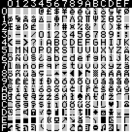
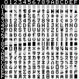
The player charsets:
 Old LCD charset (before v4.50) |
 New LCD charset (after v4.50) |
And the Recorder charset looks like this:

Code
This C snippet write a byte to the Jukebox LCD controller. The 'data' flag inticates if the byte is a command byte or a data byte.
#define DC  1
#define CS1 2
#define SDA 4
#define SCK 8

void lcd_write(int byte, int data)
{
   int i;
   char on,off;

   PBDR &= ~CS1; /* enable lcd chip select */

   if ( data ) {
      on=~(SDA|SCK);
      off=SCK|DC;
   }
   else {
      on=~(SDA|SCK|DC);
      off=SCK;
   }
   /* clock out each bit, MSB first */
   for (i=0x80;i;i>>=1)
   {
      PBDR &= on;
      if (i & byte)
         PBDR |= SDA;
      PBDR |= off;
   }

   PBDR |= CS1; /* disable lcd chip select */
}
|
Firmware size
Joachim Schiffer found out that firmware files have to be at least 51200 bytes to be loaded by newer firmware ROMs. So my "first program" only works on players with older firmware in ROM (my has 3.18). Joachim posted a padded version that works everywhere.
Tests have shown that firmware sizes above 200K won't load.
Page was last modified "Aug 7 2002" Björn Stenberg